
Semiconductors are an integral part of everyday life, in the devices and machines used frequently on a daily basis and are only increasing in importance and uses. For example, as many as 3,000 semiconductors are required for one electric car alone.

Yet there are multiple opportunities for contamination in semiconductor manufacturing, and all areas must be carefully managed to ensure that there is no opportunity for materials to become compromised.
Any contamination of semiconductor materials in manufacturing can have a serious impact on performance, with even small traces having a potentially significant effect.
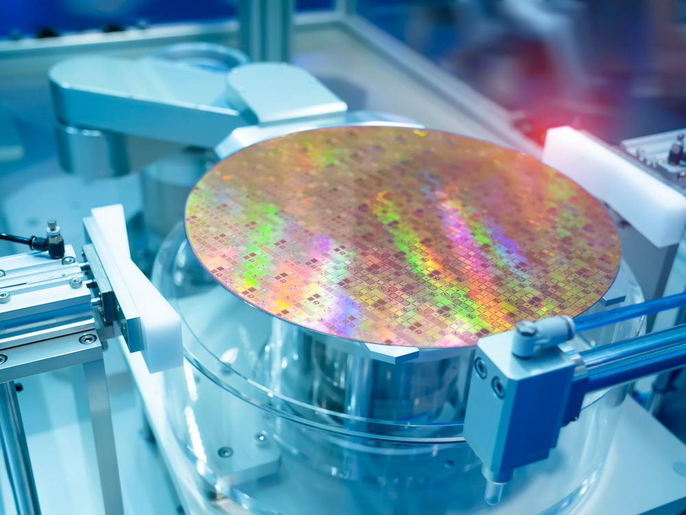
Made from one of the most abundant metalloid elements on Earth, silicon needs to be refined to 99.99999…% purity before it can be used for its large number of applications.
Materials must be robustly tested for impurities to parts per quadrillion before they can be used. The other factor that can cause problems is the presence of contaminants or defects during the fabrication phase. Every component material in a semiconductor – silicon, water, chemicals, gases, and others – must be thoroughly inspected and monitored.
Since the Covid-19 pandemic, the product supply chain has been functioning less effectively because of workplaces and production facilities shutting down around the world at various points during the last three years. Delays and shortages of raw materials and components required to produce semiconductors have also intensified demand. Missing one component or part means that a product cannot be finished. While the situation is now improving and stocks are building up again, there are extended timelines that remain for the delivery of certain devices requiring semiconductors.
With manufacturers under added pressure to meet surging demand while facing shortages of raw materials and delays in the wider supply chain, there may be a temptation to try and speed up the manufacturing of semiconductors with less stringent controls. However, any attempt to cut corners to increase the production speed can substantially reduce the quality of materials by creating more opportunities for contact with contaminants.
To ensure the quality of semiconductor materials, there must be strict environmental controls in place throughout manufacturing and fabrication, combined with rigorous testing protocols to detect and address any impurities or contaminants.
Sources of contamination in semiconductor materials
Potential contaminants of semiconductors are abundant at every stage of the manufacturing and fabrication processes. Common contaminants can come from metals, organic compounds, and ions. In addition, there are gaseous and particle impurities in gases, along with dissolved or particle impurities in chemical solutions. Sources of contaminants can come from raw materials, the environment, gases, chemicals, equipment, filter, and tubing. In fact, any contact with humans can also lead to contamination – even in cleanrooms.
“Contamination sources are everywhere,” explains Katsu Kawabata, president of Japan-based IAS Inc. “At all steps, there is a possibility of contamination. Even the cleaning process can also be a source of contamination.”
Moving from one manufacturer to the next for different materials or components in the production process also opens up opportunities for contamination and limits the ability to implement strict controls throughout.
Environmental controls play a fundamental role in reducing opportunities for contamination. In previous decades, semiconductors were fabricated using open cassettes for wafers sized between six and 18 inches. Whereas now, high-end semiconductor devices use a completely sealed cassette called Foup, restricting the ability of contaminants to come into contact with the materials.
“It’s very effective, because in the normal environment, even if you have a clean room, human beings are big particle generation sources. If someone walks around and some particles are generated, then this particle may deposit on the wafer,” adds Kawabata. “That’s why such growth of this new kind of environment is very important.”
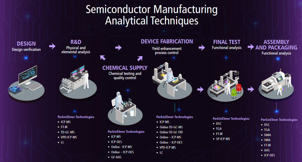
Testing solutions for semiconductors
Alongside rigorous environmental controls during semiconductor manufacturing, various testing solutions play a vital role in detecting impurities and contaminants.
XRF techniques have been commonly used to measure metallic impurities, with limitations in the effectiveness of detections. “Metallic impurities can be analysed by TRX-RF and VPD-ICP-MS. Organic compounds are analysed by GC-MS. Ionic impurities are analysed by IC,” adds Kawabata.
Depending on the device, contamination levels can vary, with Kawabata explaining that image sensor CMOS requires the lowest level of contamination controls and no destructive testing.
PerkinElmer is an established provider of systems for testing semiconductors for contaminants and impurities. The company’s NexION® 5000 is a multi-quadrupole ICP mass spec system that uses four quadrupoles. In some detection systems, octopole and hexapole are used for a reaction cell to remove interferences. Yet PerkinElmer uses its four quadrupoles for this purpose.
“The performance is quite similar in terms of interference removal, but PerkinElmer has one strong feature of this quadrupole,” says Kawabata.
“When many high-purity materials are analysed, a lot of main materials are introduced into the ICP-MS. For example, laser ablation ICP-MS introduces solid materials into the ICP-MS, and it requires the measurement of major elements. So, huge amounts of major elements are introduced into the ICP-MS, giving very high signals. If it is analysed normally, the detector of the ICP-MS is saturated. However, the PerkinElmer ICP-MS can easily reduce the sensitivity of only one element by using the reaction quadrupole.”
To learn more about PerkinElmer’s testing solutions for semiconductors, download the document below.